WellPCB Published a Guide on “10 Helpful Ways To Check Defects On Soldering PCB Board”

WellPCB, a reliable PCB & PCBA service manufacturer and provider, today published a guide on”10 Helpful Ways To Check Defects On Soldering PCB Board.”
PRESS RELEASE UPDATED: July 1, 2019
SHIJIAZHUANG, China, July 1, 2019 (Newswire.com) – WellPCB, a reliable PCB & PCBA service manufacturer and provider, today published a Guidance of 10 Helpful Ways To Check Defects On Soldering PCB Board.
The publication is available on the https://www.wellpcb.com/soldering-pcb-board.html section of the company’s website for free. It is a simple guide authored by the WellPCB technical team to help both beginners and professionals have a better understanding of Method of inspecting defects on a soldered PCB board.
“WellPCB is always working on creating and publishing articles and topics that are truly valuable to the customers that can help customers solve problems. The articles and bits of knowledge which can solve customers’ problems and needs when designing and manufacturing PCBs or seeking PCBA services; this is the value of company’s existence,” said Mr.Hommer, WellPCB General manager.
Among the key subjects on Method of inspecting defects on a soldered PCB board include:
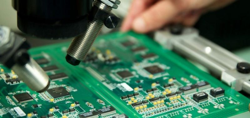
1. Identifying Common Types of PCB Soldering Defects: This section briefly describes each PCB soldering problem and its causes and solutions. It introduces Pinhole, Solder bridging, Tombstoning, Uneven hole fill, Overheated joints, Cold joints, Flux residues, Excessive. Solder, Insufficient solder, Solder skips, the causes of these, and solutions.
2. Testing methodologies for PCB soldering issues: This section details Micro-sectioning Analysis and Solder-ability Analysis.
3. Preventive Soldering Practices: This section provides an in-depth introduction to the best ways to effectively prevent weld defects: Pinhole, Solder bridging, Tombstoning, Uneven hole fill, Overheated joints, Cold joints, Flux residues, Solder skips.
Besides, The focus of this article let you familiarise yourself with common types of PCB soldering defects, how to identify them, and follow preventative soldering actions.WellPCB believes that the last chapter will interest readers. Please feel free to contact WellPCB if you have any needs or problems. There is a lot of knowledge about PCBs on the WellPCB website that can help people understand more about their needs when purchasing PCB and PCBA services.
About WellPCB
WellPCB is focusing on PCB Prototype and PCB Assembly Turnkey Services. For over ten years, WELLPCB is capable of producing 100,000 square feet of 2-32 layer PCBs and delivering over 5000 varieties monthly. WellPCB can provide quick turns to meet 24-hour delivery for double-sided PCBs, 48-hour for 4 to 8 layers and 120-hour for ten layers or higher PCBs. All PCBs products are compliant to ISO, UL, IPC Standard.
Media Contact:
Contact Person: Hommer Zhao (General Manager)
Email: [email protected]
Tel: +86-31186935221
Website: https://www.wellpcb.com
Source: WellPCB